How the latest developments have improved the performance of the sensors in our cameras.
Sensor technology has come a long way since the CCD (Charge-Coupled Device) sensors used in the original digital cameras. Today, virtually all cameras record image data with CMOS (Complementary Metal Oxide Semiconductor) chips, largely because they require less power and so are more energy efficient.
They’re also much faster at reading our image data and, because they share the same basic structure as computer microprocessors, are much cheaper to produce. They’re also more versatile since manufacturers can incorporate additional functions, such as image processing and noise reduction into the structure of the chip.
Note: Sony and Canon are the only camera manufacturers that make their own image sensors. Samsung makes image sensors for its smartphones and companies like Nikon and Fujifilm contribute to the design of sensor for particular products. However, Sony’s Semiconductor Solutions Group makes most of the sensors used in today’s cameras.
Megapixel Counts
Between about 2007, when CMOS chips became mainstream, and the early 2020s camera manufacturers used sensor size and resolution, particularly the latter, as their main marketing tools. The resulting ‘megapixel wars’ caused camera buyers to believe (often correctly at the time) that more pixels were worth paying for.
However, experience soon showed other factors play increasingly important roles in what makes a camera worth buying. Today, megapixel count per se is relatively unimportant, particularly with respect to a camera’s video capabilities, which are becoming increasingly in demand among both professional photographers and hobbyists. With each frame in a 4K video being equivalent to an 8.3-megapixel still shot, there is little need for resolutions higher than 20 and 30 megapixels.
At the same time, fewer people are printing their photos – particularly at large sizes. When you can make great-looking prints from 20-megapixel images, higher resolutions are less important than other aspects of sensor performance, like data transfer speed and the ability to record a wide dynamic range.
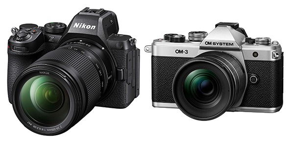
Both these cameras deliver maximum resolutions of around 20 megapixels but the sensor in the camera on the left measures 35.9 x 23.9 mm, while the on in the camera on the right is 17.3 x 13.0 mm or roughly one quarter its size. Image quality from the smaller sensor will be lower, particularly in dim lighting, because it has smaller pixels that can’t capture as much light. (Source: Nikon and OM Digital Solutions.)
Nonetheless, sensor size is still an important consideration because larger sensors have larger surface areas – which means better light-capturing capabilities. Larger photodiodes can capture more light and record more information for transfer to the camera’s image processor. This results in a wider dynamic (tonal) range with less noise – and, therefore, better picture quality.
BSI Sensors
Back-Side Illuminated (BSI) sensors made their first appearance in 2009, primarily in smartphones and compact digicams, which use smaller chips. In these chips, the normal backing material that supports the photodiode matrix is pared back and turned to face the incoming light. All the associated circuitry, which in a normal CMOS sensor covers part of the photodiode array, remains in its normal position. However, because it is now behind the photodiodes it no longer blocks the incoming light so the chip’s light absorption is increased.
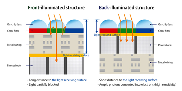
These diagrams show the structural differences between front side illuminated (FSI) and back side illuminated (BSI) CMOS sensors. (Source: Sony Semiconductor Solutions.)
Parallel developments have also allowed designers to incorporate more analog-to-digital converters (ADCs) on the chip itself and place them closer to the actual pixels. This results in faster readouts with a significant reduction in read noise.
BSI arrived in large sensors in 2014 but, since the wiring on the larger chips takes up less space relative to the pixels, they provided proportionally fewer improvements to image quality. Nonetheless, moving the wiring behind the pixel provided space for more complex circuitry, which allowed for an increase in the number of ADCs and increase in readout speed without increased noise.
Stacked Sensors
The first stacked CMOS image sensor, the Exmor RS, was introduced by Sony in August 2012. Whereas conventional back-illuminated CMOS image sensors had a layer that carried both the pixel and circuit sections with a ‘supporting substrate’ underneath, in a stacked sensor, the pixel layer and the logic circuit are separated to position one layer above the other. This allows each layer to be optimised for its specific function.
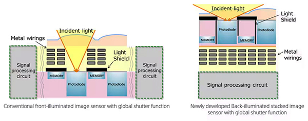
These diagrams show the structural differences between a conventional CMOS sensor and a stacked image sensor with a global shutter function. (Source: Sony Semiconductor.)
Separating the pixel and circuit layers means the photodiodes can be larger per unit area and, therefore, capture more light per unit of exposure. The circuit layer also covers the entire chip, allowing more space for signal processing and resulting in higher image quality and enhanced capabilities at lower power consumption levels. In addition, the distance the image data has to travel to reach the image processor is shorter, resulting in much faster processing speeds.
Dual Pixel CMOS AF
Dual Pixel CMOS AF is a completely different technology, introduced by Canon in 2013, mainly to ensure fast, accurate and smooth autofocus during Live View and video shooting. Each pixel on the image sensor is split into two light-sensing photodiodes that capture slightly different views of the image. A processor analyses the phase difference between these two images to calculate if the image is in focus and in which direction the lens needs to move.
![]()
This series of diagrams shows how Canon’s Dual Pixel CMOS AF system works. (Source: Canon.)
Both photodiodes are also used for image capture so the system still delivers excellent image quality without compromising autofocus performance. An enhanced version of the system, Dual Pixel CMOS AF II, was introduced in 2020, incorporating EOS intelligent Tracking and Recognition Autofocus (EOS iTR AF X), which is based upon Deep Learning AI technology. Dual Pixel CMOS AF II is now widely used across the EOS R System and Cinema EOS lines.
Dual Pixel Intelligent AF arrived in 2024 in the EOS R1 and EOS R5 Mark II cameras, providing further refinements to detection and tracking capabilities and enabling the introduction Action Priority AF. This allows the camera to track actions commonly seen in certain sports and automatically shift the focus to the area where the action is taking place. Both cameras are also equipped with a DIGIC Accelerator, which boosts the volume of data the camera can process and enables features such as faster electronic shutter speeds, simultaneous recording of stills and video and a significant reduction in rolling shutter distortion compared to earlier cameras.
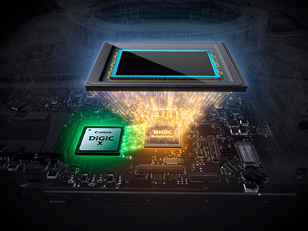
The new DIGIC Accelerator chip in Canon’s professional cameras significantly increases image processing speeds. (Source: Canon)
The system was further enhanced in the EOS R1 with Cross Type AF, allowing the sensor to detect phase differences not just vertically, but also horizontally at the same time. This improves focusing accuracy and speed in low-light and low-contrast situations and delivers even more stable AF performance in the continuous shooting mode.
Global Shutters
Sony is at the forefront of developments in global shutter technology, introducing it in the α9 III camera in late 2023. Unlike traditional focal plane shutters that capture an image by scanning the sensor from top to bottom, a global shutter captures the entire frame at once.
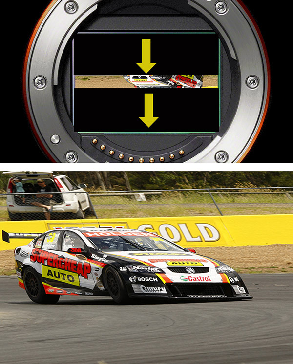
Focal plane shutters have two blinds that open as a travelling slit, which exposes the sensor line by line, starting from the top and progressing to the bottom. When subjects are moving quickly, their position changes during the exposure and the small delay from line to line, results in a laterally distorted image (lower section of the illustration above).
Global shutters eliminate rolling shutter distortion in fast-moving scenes and when panning by exposing all sensor photodiodes at the same time. They’re a game-changer for sports, action, and also help wedding photographers who require precision with speed.
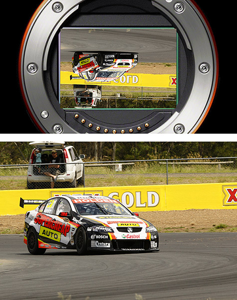
A global shutter exposes all the pixels of the array at the same time so there is no image distortion.
Global shutters also allow electronic flashes to be used at high shutter speeds, although there are still issues associated with synchronising the flash to fire when the shutter is wide open, particularly at shutter speeds higher than about 1/500 second. With faster shutter speeds, exposures may only capture part of the flash output so the flash timing must be adjusted to precisely align the shutter with the peak brightness of the flash curve.
Capturing Colour
Almost all image sensors are equally sensitive to all wavelengths of light, which means they can’t discriminate between colours. In order to record the intensities of the three main colour bands – red, green and blue – most sensor manufacturers place a colour filter array over the sensor.
The most commonly-used filter is the Bayer matrix, which consists of a square grid of coloured patches that fits over the chip, with each patch covering a single photodiode. There are twice as many green patches as either red or blue patches, as shown in the diagram below.
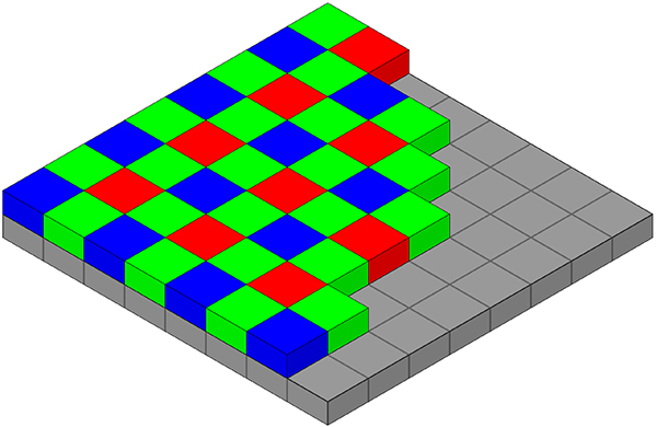
This diagram shows a Bayer filter array overlaid on the basic photodiode grid that makes up a typical image sensor. (Source: Cburnett, CC BY-SA 3.0, via Wikimedia Commons.)
The reason for this is that human vision is most sensitive in the green band of the visible spectrum so the filter roughly matches the sensitivity of our eyes. Since each pixel is filtered to record only one of three colours, to obtain a full-colour image the data from all the filters must be interpolated to bring in data from the surrounding red, green and blue filtered pixels in order to estimate the colour values for each particular pixel.
This can be done in-camera to produce a JPEG or TIFF image, or outside the camera using the raw data directly from the sensor and raw file conversion software. Different algorithms use different amounts of computing power, which results in varying quality in the final images. Camera and software manufacturers are continually fine-tuning their demosaicing algorithms to deliver better colour accuracy.
![]()
The filter array pattern used in Fujifilm’s X-Trans sensors. (Source: Fujifilm.)
Fujifilm has developed a variation on the traditional Bayer filter array, which is based upon a 6×6 pattern in which all three colours are used in each row of filter patches, instead of the red and blue patches appearing in alternating rows as they do in a Bayer filter. The new X-Trans sensors were introduced in the X-Pro camera, which was launched in 2012.
Fujifilm claims the irregular pattern reduces the likelihood of moiré (cross-pattern interference) and removes a need for a low-pass filter that lowers image resolution. The first three generations of X-Trans sensors were front-illuminated, with subsequent generations being backside illuminated to improve noise levels and image quality. Stacked layer, back illuminated X-Trans CMOS 5 HS sensors were introduced in 2022, with a high resolution of 40.2 megapixels.
A more radical approach to colour creation was developed by Foveon, Inc., back at the beginning of the 21st Century. Instead of covering a CMOS sensor with a filter, it uses a sensor consisting of three, vertically stacked photodiodes, each of which is sensitive to a different band in the spectrum.
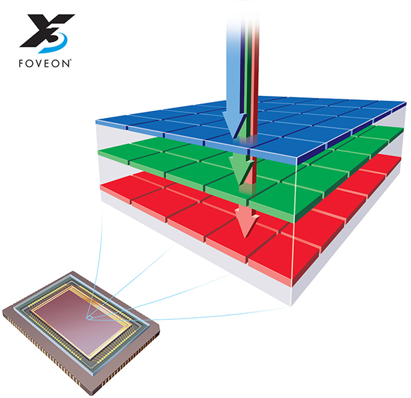
This diagram shows the layered structure of the Foveon X3 sensor.
Foveon was purchased by Sigma and the X3 chip was first used in the Sigma SD9 DSLR camera, which was launched in 2002. These sensors have subsequently been used in the SD10, SD14, SD15, SD1 (including SD1 Merrill), the original mirrorless compact Sigma DP1 and Sigma DP2 in 2008 and 2009 respectively, the Sigma dp2 Quattro series from 2014, and the Sigma SD Quattro series from 2016. Sigma discontinued the last cameras to use the Foveon X3 sensor in 2022 and has not released any cameras since then with this sensor.
While theoretically the Foveon X3 sensor should be able to produce ‘purer’ colours than Bayer filtration, in practice, the individual layers in a Foveon sensor don’t respond as sharply to the respective colours so the colour data requires ‘aggressive’ processing to deliver good results. Images captured can also be subject to increased colour noise in low-light situations.
In 2021, Sigma was working on developing a new Foveon sensor but the company reported a critical flaw was found and it had to restart development from scratch. The second stage of prototyping the new full frame Foveon sensor was reported in February 2022 but as of mid-2025, an updated Foveon X3 sensor has yet to be produced.
Article by Margaret Brown
See Margaret’s Photo Review photography guides